menumenu
University of New Orleans Logo University of New Orleans Logo

Hamburger Aux Menu

  • Maps & Directions
  • For Current Students
  • For Faculty & Staff
  • For Alumni
  • For Parents
  • Employment Opportunities
  • Give Now
  • Privateer Sports

Hamburger Menu

  • University of New Orleans Logo
  • Summer Session
  • Accepted Students
  • Admissions
    • Visit Campus
    • Undergraduate Admissions
    • Graduate Admissions
    • Financial Aid
    • Tuition and Fees
    • Scholarships and Awards
  • Academics
    • Academics Home
    • Undergraduate Programs
    • Graduate Programs
    • General Education
    • Professional and Continuing Education (PaCE)
    • Online Degree Programs
    • Service Learning
    • Study Abroad
  • Colleges
    • Business Administration
    • Engineering
    • Liberal Arts, Education and Human Development
    • College of Sciences
    • School of the Arts
    • School of Education
    • School of Naval Architecture
    • Hotel, Restaurant & Tourism
    • School of Interdisciplinary Studies
    • The Graduate School
  • About UNO
    • About UNO
    • At A Glance
    • Office of the President
    • Administrative Offices
    • Mission & Vision
    • History
    • University Advancement
    • Alumni
  • Research
    • Research Home
    • Faculty & Staff Research
    • Student Research
    • Collaborate with UNO
    • Office of Research
  • Student Life
    • Student Life Home
    • Campus Safety
    • On Campus Housing
    • Campus Dining
    • Recreation & Fitness
    • Student Health
    • Campus Hangouts
    • Get Involved
UNO Logo
  • university of new orleans
  • advanced materials research institute (amri)
  • amri facs
  • analysis
  • scanning electron microscope
IN THIS SECTION
  • Analysis
    • Microscopy
    • Magnetism
    • X-ray Powder Diffraction
    • Profiler
    • Thermal Analysis
    • Visit Us
    • Apply to UNO

JSM-5410 Scanning Electron Microscope

sem/eds

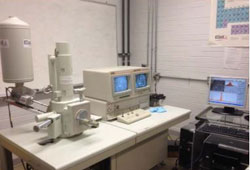
Scanning Electron Microscope (SEM) is a type of electron microscope that produces images of a sample surface by scanning samples with a focused beam of electrons. The JEOL JSM-5410 SEM in our lab is capable of imaging sample surface morphologies by using secondary electrons or back-scattered electrons, equipped with an Energy Dispersive X-ray Spectrometer (EDS) for chemical analysis. With robust W filament, the SEM is capable of characterizing different materials, such as semiconductive, geological, biological, and composite materials.

Specifications and capabilities of JSM-5410 SEM

  • Resolution: 3.5 nm (Accv. 30 kV, WD = 6 mm, secondary electron image)
  • Magnification: x15 (WD = 48 mm) to 200,000 (25 steps)
  • Image modes:
  • Secondary electron image (SEI) HV Mode
  • Backscattered electron image (BEI) HV Mode
  • Backscattered electron image (BEI) LV Mode
  • Accelerating voltage: 0.5 to 30 kV
  • EDAX Genesis Software: Point, line, and area EDS analysis as well EDS mapping

User Rates

Rates will be based on an hourly or per sample basis and will be decided after consultation with the customer.

Assisted Use: $20/hr.*


Training: $25/hr.


Self-Use: $10/hr.


Consumables charged at cost.

Contact Us

Dr. Weilie Zhou
Email: wzhou@uno.edu

Sample Data

Sample Data
  • University of New Orleans Logo
  • 2000 Lakeshore Drive New Orleans, LA 70148
  • 888-514-4275
  • Additional Contacts

Learn

  • Admission Information
  • Programs of Study
  • Scholarships and Awards
  • Tuition and Fees

Experience

  • International Center
  • Our Campus
  • Student Life
  • Accessibility

Connect

  • All Social
  • University Calendar
  • Español - Tiếng Việt
Request Info
Apply
Visit
Give
© 2024 University of New Orleans Emergency Preparedness UL System Non-Discrimination Campus Crime Stats Title IX & Power Based Violence